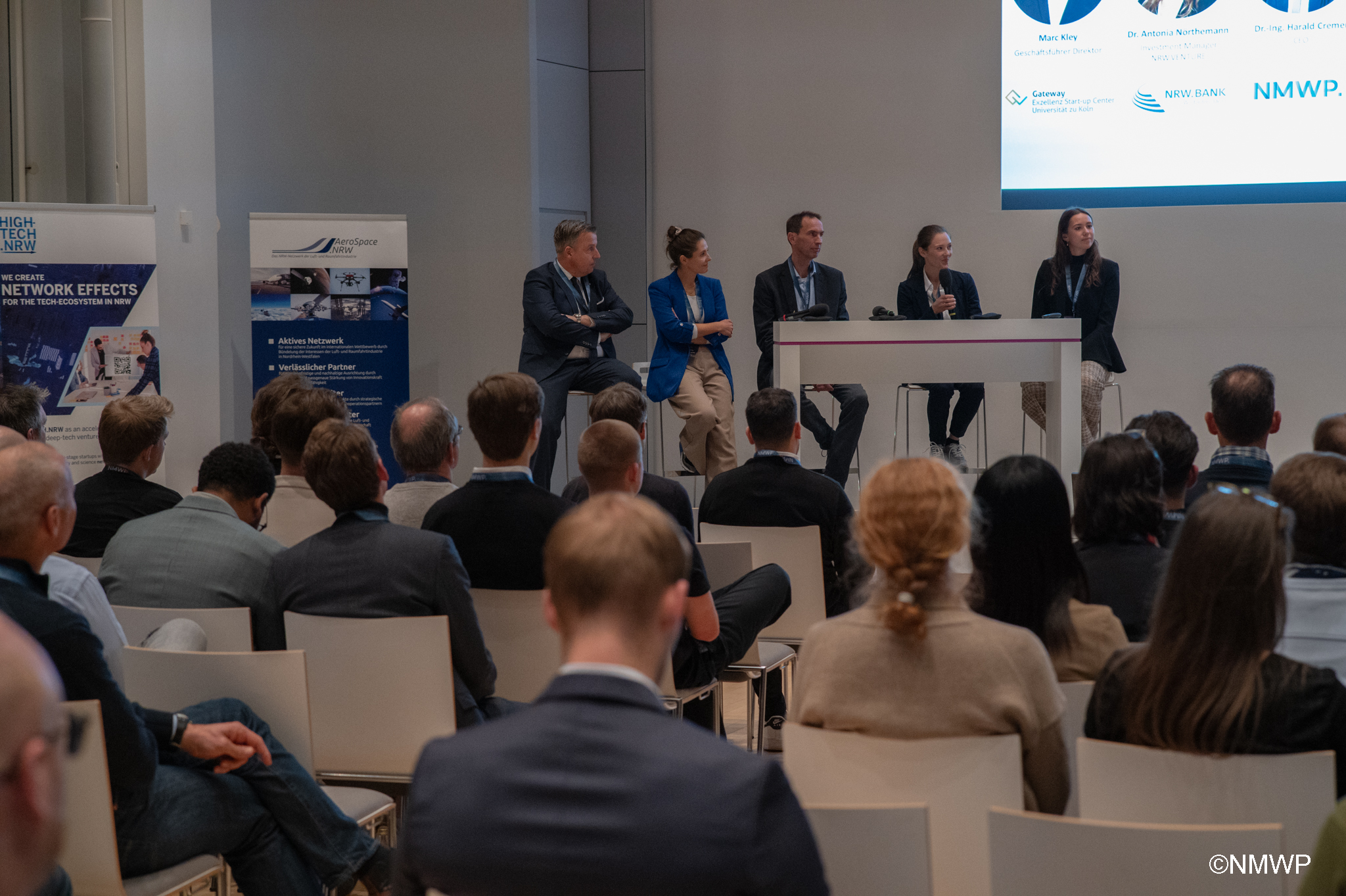
Nothing less than a semiconductor revolution

Next Level Epitaxy

Lower deposition temperatures, lower energy and process gas consumption, faster production and combination of new materials for wide-bandgap semiconductors. ELEMENT 3—5 leaps epitaxy to the next level.

up to
90%
energy savings
up to
10x
higher throughput
up to
700%
more productivity

ACCELERATOR 3500K

The new perspective for wide-bandgap semiconductors: With vertically integrated manufacturing and lower process temperature than conventional techniques such as MOCVD/MBE. For new possibilities from LED-lighting to high-power electronics.
Learn more
Flexible and successful

Maximum efficiency

Novel design combined with our innovative in-line manufacturing concept is the basis for scalable mass-production and significant increase in efficiency.

view into wafer production
New approach,
new possibilities

Vertically integrated production

ELEMENT 3—5 sets new standards in the manufacturing process mode of semiconductors. For this purpose, we set up the wafer vertically and thus achieve the greatest possible homogeneity and particle-free production.

three wafer one surface
LowER deposition temperature, lowER cost

Highest quality

Our unique process method enables deposition of monocrystalline structures of the highest quality at temperatures below 300 °C. Thus, the production is much more environmentally friendly, energy-saving and also more cost-efficient than the conventional process techniques.

view into semiconductor produciton
LowER temperature,
more choices

Leveraging new potentials

We are opening up completely new opportunities for the semiconductor industry. Due to process temperatures below 300 °C, temperature-sensitive substrates can be deployed, materials beyond the 3rd and 5th main groups can be deposited and new stacks can be built in.

a person in a laboratory outfit holds a wafer

Greener & cleaner

ELEMENT 3—5 technology relies on intelligent plasma and renders the use of toxic gases in semiconductor production obsolete. Operation and maintenance is much easier and, together with energy savings of up to 90 percent in production, we significantly reduce the environmental impact.

Learn more

About Element 3—5

ELEMENT 3—5 [Element three to five] sets new standards in semiconductor manufacturing. As a high-tech company from the Aachen region, we develop innovative high-performance production systems of wide-bandgap semiconductors. More cost-effective, more functional, more sustainable. With our products and services, we enable our partners to bring their innovations to market faster, more efficiently and in a more environmentally friendly way.
Learn more
The latest from the world of ELEMENT 3—5

ELEMENT 3-5 breaks new ground again – EPIWIN project successfully launched

Although ELEMENT 3-5 GmbH is already breaking new ground in semiconductor technology with the introduction of the Next Level Epitaxy, the company is pleased to be contributing another significant building block to changing semiconductor production with the launch of the EPIWIN joint project. EPIWIN stands for "epitaxy with integrated nanostructuring". The project aims to combine the Next Level Epitaxy of ELEMENT 3-5 GmbH with laser structuring processes in the sub-μm and ~10μm range in order to enable the production of low-dislocation layers in finished, isolated dies. This method will be much more cost-effective and also more environmentally friendly than the conventional method for the production of semiconductor components, which requires the use of several systems between which the wafer is repeatedly transported with an increased risk of contamination - in some cases even at different locations or outsourced to suppliers. In order to limit the risk of contamination to some extent, wafer transport is therefore carried out in vacuum-sealed disposable packaging in the conventional production sequence, which creates a large amount of packaging waste. This is not the case with EPIWIN: The integration of structuring and epitaxy into a system concept opens up the possibility of assembly line production, which, in addition to reducing the reject rate, also halves energy consumption and reduces environmental pollution by a factor of more than three. A significant cost reduction is a matter of course. In addition to ELEMENT 3-5 GmbH, which has also taken on the role of project coordinator, the project partners in the EPIWIN project are the Fraunhofer Institute for Laser Technology ILT and Innolite GmbH. Associated partner is Coherent Laser Systems GmbH. Thanks to Fraunhofer ILT's many years of experience in the field of laser structuring, the know-how of ELEMENT 3-5 GmbH in the field of low-temperature epitaxy and the expertise of Innolite GmbH in the production of high-precision optical elements, the necessary competencies for this project are excellently developed. The "EPIWIN" project is funded as part of the ERDF/JTF programme NRW 2021-2027 with the funding measure "Innovation Competition Industry.IN.NRW". The funds are provided by the Ministry of Economic Affairs, Industry, Climate Protection and Energy of the State of North Rhine-Westphalia, co-financed by the European Union. The start of the joint project was May 1, 2024. The term is 3 years.

Questions?
Just contact us!
We are delighted to answer your questions.
Contact us
By clicking “Accept”, you agree to the storing of cookies on your device to enhance site navigation, analyze site usage, and assist in our marketing efforts. View ourPrivacy Policyfor more information.